ARTICLE AD BOX

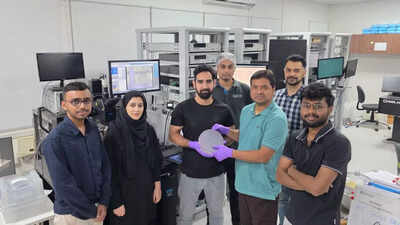
Mayank Shrivastava (third from right) holding a representative power device 8” wafer, with some of his PhD students who work on various aspects of GaN Power and RF technology (Photo credit: IISc)
BENGALURU: Researchers from the Indian Institute of Science (IISc) have reported a breakthrough in the design of gallium nitride (GaN) power transistors, a development that could help accelerate the use of the material in electric vehicles (EVs), data centres and renewable energy systems.Gallium nitride, or GaN, is seen as a successor to silicon in high-power electronics because it can reduce energy losses sharply and shrink the size of power converters by almost three times. Yet commercial adoption has been cautious. “Existing devices rely on a p-GaN gate that switches on at a low threshold voltage of about 1.5 to 2 volts and begins to leak current beyond 5 to 6 volts, limiting reliability in demanding applications.
A team from the Department of Electronic Systems Engineering at IISc set out to understand the physics behind this behaviour,” IISc said.In a two-part study, the team examined how the gate structure controls the flow of current and what determines the crucial threshold voltage. Prof Mayank Shrivastava, who led the work, said the researchers first established the link between the depletion state of the p-GaN layer, tiny leakage pathways and the moment when the transistor turns on.
“Small leakage paths can decide the entire turn-on behaviour,” he noted.The scientists created several experimental gate variants and combined electrical measurements with modelling and microscopy. They found that when the p-GaN layer is only partly depleted, minute charges accumulating at a key interface can trigger the device to switch on early. Suppressing that accumulation forces the transistor to turn on later at a higher and safer voltage.Using these insights, IISc said, the group designed new metal-based gate stacks that cut leakage by up to 10,000 times and improved the stability of the threshold. Gate breakdown voltages reached about 15.5 volts, a significant jump over current designs.“In the second phase, the team developed an integrated aluminium–titanium oxide gate stack, a patented concept that blocks unwanted charge injection and enables a high-threshold mode similar to silicon Mosfet devices.
The resulting transistors achieved threshold voltages above 4 volts while retaining strong control and robustness,” IISc said.Rasik Rashid Malik, the doctoral researcher and lead author, said the advance could hasten GaN use in EV power converters, server power supplies and renewable energy inverters where reliability is critical.The researchers are now looking to scale the technology through govt support and industry partnerships. Shrivastava said achieving high threshold voltage together with low leakage was essential for the next phase of GaN adoption, adding that the team had addressed a long-standing barrier for the electronics sector.

 5 days ago
4


 English (US) ·